DRAM Scaling with High Work Function Electrode Materials
By
Tejinder Singh
Chief Technology Officer
Eugenustech
Share this content
September 16, 2025
5
minute read
Dynamic Random-Access Memory (DRAM) remains a cornerstone of modern computing, powering everything from smartphones to servers. DRAM is the essential component in High-bandwidth memory required for the most advanced AI chips. As the industry pushes toward higher density and performance, DRAM scaling faces one persistent challenge: capacitor leakage. Leakage directly impacts retention time, refresh cycles, and ultimately device reliability. The race to extend DRAM scaling into 4F² cells and 3D-DRAM architectures depends heavily on finding new materials that balance capacitance with leakage control.
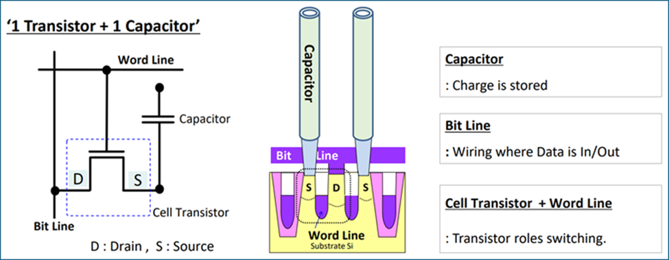
DRAM Unit Cell
A DRAM unit cell is a 1T-1C structure as shown in Figure 1, consisting of one transistor and one capacitor:
Capacitor: This component stores the electrical charge that represents a bit of data. A stored charge is a '1', and no charge is a '0'.
Transistor: This acts as a switch, controlling the flow of data to and from the capacitor.
Word Line: This activates the transistor, allowing access to the cell.
Bit Line: This is the wiring used for data input and output.
Figure 1: DRAM Unit Cell (Source: Samsung Short Course IEDM, 2024)
DRAM Refresh Cycle
Figure 2 illustrates how leakage current in DRAM capacitors affects data retention over time. In an ideal low-leakage cell (green curve), the stored voltage decays slowly, remaining above the data loss threshold for the full refresh interval (e.g.,64 ms). In contrast, a high-leakage cell (red dashed curve) discharges more rapidly, crossing the threshold well before the refresh limit, which leads to data corruption unless refresh cycles are made more frequent. This highlights why reducing leakage in DRAM capacitors is essential — not only to maintain retention time but also to minimize refresh overhead and power consumption.
Figure 2: Effect of leakage on DRAM retention
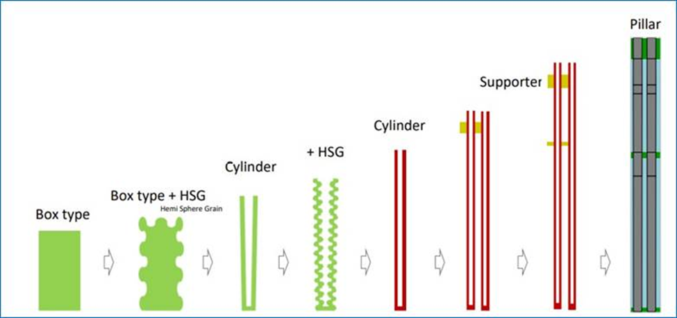
Evolution of DRAM Capacitor
Figure 3 shows the evolution of DRAM capacitor as the technology has scaled to achieve higher capacitance within smaller cell areas. Since DRAM density continues to grow while cell size shrinks, DRAM capacitors have progressively scaled to maximize effective surface area while keeping the cell area minimal. This evolution shows how capacitor design innovations—moving from box to pillar structures—have been critical enablers for DRAM scaling. Each step solves the dual challenge of maintaining capacitance while fitting into ever-shrinking cell sizes.
In the previous generation, DRAM capacitor was shaped in cylinders with Supporter. As the aspect ratio increased to >50:1, mechanical stability became an issue. Support structures were introduced to prevent collapse during processing. Most recent DRAM technology has Pillar capacitor, using stacked or “pillar” capacitors, enables even higher aspect ratios and surface area, making it suitable for advanced DRAM nodes and 3D-DRAM architectures.
Figure 3: DRAM Cell Capacitor Scaling (Source: Samsung Short Course IEDM, 2024). Inset shows DRAM unit cell (6F2) with cylindrical capacitor (Source: TechInsights analysis of Samsung 1x technology node).
Root cause of Leakage in Advanced DRAM
Leakage current in metal–insulator–metal (MIM) capacitors is dictated through the equation.
J represents the leakage current, which is the unwanted flow of charge out of the capacitor.
tox: This is the dielectric thickness. A thinner dielectric layer can lead to a higher leakage current.
EB: This likely represents the barrier height or band offset. A higher barrier height helps to reduce leakage.
meff: This is the effective mass of the tunneling electron, a property of the material.
Based on tunneling current equation, leakage arises from multiple mechanisms:
Direct tunneling through thin dielectrics due to insufficient band offsets.
Defect-assisted conduction from oxygen vacancies and interface states.
Grain boundary conduction in crystalline high-k oxides.
Thermally activated leakage paths under high electric fields.
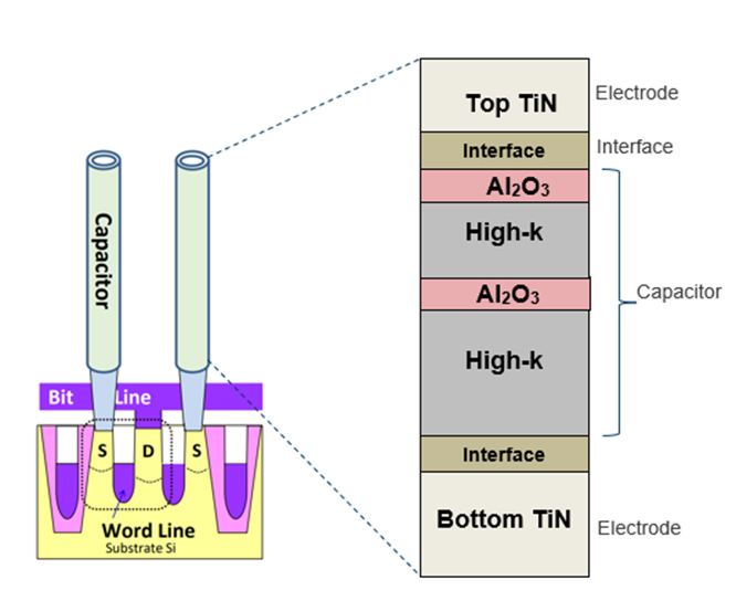
Approaches for Leakage Reduction
Figure 4 shows how each layer impacts leakage in DRAM capacitor. Multiple strategies have been investigated to solve the leakage problem in DRAM as summarized below:
Figure 4: Radial cross of DRAM Capacitor showing the MIM Capacitor
High WF Metals: Use high work function metals for the capacitor electrodes, which provides a higher band offset to reduce leakage.
Higher-k Dielectrics: Employ higher-k dielectric materials, such as replacing ZAZ with TiO2, to improve capacitance and reduce leakage
Interface Control: Control the interface between the electrode and the dielectric to reduce roughness and minimize defects and vacancies, which can act as leakage paths.
High Bandgap "Blocking" Layers: Introduce high bandgap blocking layers like NbO, MoO, or NbN to further prevent charge leakage.
Grain Boundary and Phase Control: Engineer the grain boundaries and phases of the crystalline high-k dielectric to improve its properties and reduce leakage.
Dielectric Thickness & Stack Stability: Maintain the stability and optimize the thickness of the dielectric stack to improve charge conservation.
Focusing on option #1, TiN electrodes paired with high-k dielectrics such as HfO₂, ZrO₂, or Al₂O₃ are widely used in today’s most advanced DRAM technology. However, TiN electrodes have inherent limitations:
Work function (WF ~4.3 eV) is too low to suppress leakage when scaled dielectrics are used.
Sheet resistance (>1000 Ω/sq at 50 Å) constrains electrode thickness, increasing leakage risk at reduced thickness.
These limitations drive the urgent need for next-generation electrode materials.
Eugenus's Solution: High Work Function Materials
To solve the leakage problem, the industry has explored a variety of new materials for DRAM capacitor electrodes as summarized in Table 1.
Table 1: Candidate materials for High Work Function Materials for DRAM Capacitor Electrode
Material
Advantages vs. TiN
Challenges
Process
Ru
Lower resistivity than TiN, compatible with high-k dielectrics (HfO₂, ZrO₂), good conformality in ALD
Higher cost, ALD process not mature, etch selectivity issues
ALD/PVD
Ir (Iridium)
Excellent barrier properties, stable interface with high-k
Expensive, difficult etch, less mature integration history in DRAM
PVD
RuO₂
Reduces leakage via better interface with dielectric, potential oxygen reservoir
Higher resistivity than Ru, requires precise stoichiometry control
Slightly higher resistivity than TiN, ALD process complexity
ALD/PVD
MoN
Good barrier properties, compatible with ALD
Higher resistivity than TiN, integration immaturity
ALD/PVD
W (Tungsten)
Excellent conductivity, existing BEOL integration
Poor oxidation resistance, reacts with high-k unless barrier used
CVD
Pt (Platinum)
Very low leakage, inert interface
Very high cost, etch difficulty, contamination concerns
PVD
TaN
Better oxidation resistance than TiN
Higher resistivity, potential work function mismatch
ALD/PVD
VN
Higher WF, Lower oxygen diffusivity
Integration with High-k, particles
ALD
While several candidate materials exist, VN (Vanadium Nitride) stands out as the most promising.
Eugenus has developed a Metal ALD (Atomic Layer Deposition) system called Sierra, which is designed for high work function, low resistivity materials like VN. Compared to the traditional TiN (Titanium Nitride) electrode material, VN offers significant advantages:
Higher Work Function: VN has a work function greater than 5 eV, while TiN is 4.3 eV. This higher work function leads to lower leakage (Figure 4).
Figure 5: Leakage current as a function & Work function showing comparison of TiN & VN
Lower Resistivity: VN has a resistivity of less than 100 Ohm/Sq at 50 Angstroms, whereas TiN's is greater than 1000 Ohm/Sq at the same thickness.
Lower Leakage: VN provides lower leakage compared to the TiN baseline at matched capacitance.
Excellent Step Coverage: Both TiN and VN maintain over 98% step coverage, which is a critical requirement for the high aspect ratio structures in DRAM.
Sierra is designed for applications that demand high aspect ratio step coverage – from capacitor electrodes in memory to barrier layers in advanced logic devices. It supports a wide range of materials, including TiN, TSN, and VN, with superior station-to-station repeatability.
Implications for DRAM Scaling
By addressing the leakage bottleneck, VN/TiN electrodes enable:
Longer retention times, reducing refresh overhead and improving energy efficiency.
Scalable electrode thickness, maintaining conductivity in ultra-scaled capacitors.
Integration into 3D-DRAM, where leakage challenges are compounded by extreme aspect ratios.
These new materials are essential for the future of DRAM, as the industry evolves from 6F2 to more advanced 4F2 and 3D-DRAM structures, which require new materials for scaling, performance, and cost. The development of these new materials and processes is crucial for advancing DRAM technology. VN/TiN provides a manufacturable, ALD-compatible path forward.